Скачать с ютуб EXPERIMENT NO 1 || VI CHARACTERISTICS OF SI DIODE AND MEASUREMENT OF STATIC AND DYNAMIC RESISTANCE в хорошем качестве
EXPERIMENT NO 1 || VI CHARACTERISTICS OF SI DIODE AND MEASUREMENT OF STATIC AND DYNAMIC RESISTANCE
3 года назад
Скачать бесплатно и смотреть ютуб-видео без блокировок EXPERIMENT NO 1 || VI CHARACTERISTICS OF SI DIODE AND MEASUREMENT OF STATIC AND DYNAMIC RESISTANCE в качестве 4к (2к / 1080p)
У нас вы можете посмотреть бесплатно EXPERIMENT NO 1 || VI CHARACTERISTICS OF SI DIODE AND MEASUREMENT OF STATIC AND DYNAMIC RESISTANCE или скачать в максимальном доступном качестве, которое было загружено на ютуб. Для скачивания выберите вариант из формы ниже:
Загрузить музыку / рингтон EXPERIMENT NO 1 || VI CHARACTERISTICS OF SI DIODE AND MEASUREMENT OF STATIC AND DYNAMIC RESISTANCE в формате MP3:
Если кнопки скачивания не
загрузились
НАЖМИТЕ ЗДЕСЬ или обновите страницу
Если возникают проблемы со скачиванием, пожалуйста напишите в поддержку по адресу внизу
страницы.
Спасибо за использование сервиса savevideohd.ru
EXPERIMENT NO 1 || VI CHARACTERISTICS OF SI DIODE AND MEASUREMENT OF STATIC AND DYNAMIC RESISTANCE
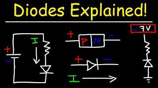
#Diode_Characteristics #Methodist_College_Of_Engineering_and_Technology 1.1 AIM: To Obtain and Plot the Forward and Reverse VI Characteristics of PN Junction Diode [Si, Ge] and to determine the Static and Dynamic Resistances. 1.2 APPARATUS: S.NO DESCRIPTION RANGE QUANTITY 1. Regulated Power Supply 0-30 VDC, 2 A 1 2. Voltmeter 0-20 VDC (Digital Meter) 1 3. Ammeter 0-50 mA, 10-100 µA (Digital Meter) 1 1.3 COMPONENTS: S.NO DESCRIPTION RANGE QUANTITY 1. Si Diode 1N4007 1 2. Ge Diode OA 79 1 3. Resistors 1 KΩ 1 4. Bread Board - 1 1.4 THEORY: When one half of a piece of semiconductor material is doped with a p-type impurity and the other half with an n-type impurity, a p-n junction is formed, and a potential barrier develops. The terminal brought out from the p-type is the anode and the terminal brought out from the n-type is the cathode. When the anode is connected to the positive terminal of the battery, and the cathode to the negative terminal, the diode is forward-biased, its potential barrier lowered, and a large current flow is restricted by the introduction of a series resistor. The barrier is merely lowered and does not disappear. When forward biased, the diode resistance will be quite small of the order of tens of ohms. When the polarities are reversed, the diode will be reverse-biased and blocks forward current because the potential barrier is increased, and the diode resistance is large of the order of hundreds of kilo-ohms. However, a reverse saturation current of the order of a few micro-amps will flow due to carrier generation. The property of allowing large forward currents and blocking reverse currents (neglecting the reverse saturation current) and the large reverse breakdown voltages (tens to hundreds of volts) makes the device useful as a rectifier that converts AC voltage to pulsating DC voltages. In a forward bias, the diode conducts when the forward voltage VF across the diode exceeds Vγ, the cut-in voltage: The cut-in voltage Vγ is defined as the voltage at which 1% of rated current flows. For example, for the 1N4007 diode, the rated current is 1A and therefore the cut-in voltage will be the voltage across the diode when 1000mA × 1/100= 10mA current flows. The cut-in voltage for the Germanium diode is approximately 0.2 Volts and for the Silicon, the diode is approximately 0.6 Volts. 1.5 PROCEDURE: 1.5.1 SILICON DIODE 1.5.1.1 SILICON DIODE FORWARD BIAS • Connect the circuit according to the schematic in Fig. 1. • Increase the voltage in steps of 2V up to 8V and then at 16V, 20V, 25V and 30V while noting down in Table 1 the corresponding forward current. • Plot the curve of VF vs IF on a graph paper and calculate the static forward resistance and dynamic forward resistance. 1.5.1.2 SILICON DIODE REVERSE BIAS • Now connect the circuit according to the schematic in Fig 2. • Increase the voltage in steps of 2V up to 8V and then at 16V, 20V, 25V and 30V while noting down the reverse current in Table 2. • Plot the curve of VR vs IR on a graph paper and calculate the static and dynamic Reverse Resistance. 1.6 CIRCUIT DIAGRAM Figure 1 Schematic for forwarding Bias PN Junction Diode Supply Voltage (VS) in Volts VF (Volts) IF (mA) 0.15 0.15 0.181 Micro 0.30 0.296 3.968 Micro 0.45 0.407 0.043 Milli 0.6 0.462 0.138 Milli 0.75 0.492 0.258 Milli 0.9 0.511 0.389 milli 1.05 0.525 0.525 Milli 1.20 0.536 0.664 Milli 1.35 0.545 0.805 Milli 1.50 0.552 0.948 Milli 1.65 0.559 1.091 Milli 1.8 0.565 1.235 Milli 1.95 0.57 1.38 Milli 2.10 0.575 1.525 Milli 2.25 0.579 1.671 Milli 1.8 CALCULATIONS FORWARD BIAS REVERSE BIAS 1.9 RESULT: The V-I characteristics of the given p-n junction diode in forward bias and reverse are determined. 1. Cut in Voltage of PN Junction Diode 1N4007 is = Volts; = Milli Volts 2. Static Forward Resistance 1N4007 is = Volts; = Ω 2. Dynamic Forward Resistance 1N4007 is = Volts; = Ω 4. Static Reverse Resistance 1N4007 is = Volts; = Ω 5. Dynamic Reverse Resistance 1N4007 is = Volts; = Ω Static Resistance [VF/IF] Static Resistance [VR/IR] Dynamic Resistance[∆V/∆I] = = V2-V1/ I2-I1 Dynamic Resistance[∆V/∆I] = |V2|-|V1|/ |I2|-|I1| YouTube: / maharshisanandyadav Facebook Page: / hometuitionsece Google Form: Registration https://www.google.com/url?q=https%3A... Website: https://sites.google.com/view/tmsytut...
Comments