Скачать с ютуб Transistor working in tamil в хорошем качестве
Transistor working in tamil
4 года назад
Скачать бесплатно и смотреть ютуб-видео без блокировок Transistor working in tamil в качестве 4к (2к / 1080p)
У нас вы можете посмотреть бесплатно Transistor working in tamil или скачать в максимальном доступном качестве, которое было загружено на ютуб. Для скачивания выберите вариант из формы ниже:
Загрузить музыку / рингтон Transistor working in tamil в формате MP3:
Если кнопки скачивания не
загрузились
НАЖМИТЕ ЗДЕСЬ или обновите страницу
Если возникают проблемы со скачиванием, пожалуйста напишите в поддержку по адресу внизу
страницы.
Спасибо за использование сервиса savevideohd.ru
Transistor working in tamil
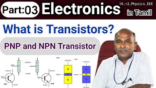
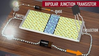
Transistor working Principle of Operation. There are different types of transistor available in the market, but for sake of understanding, we will consider a common emitter mode of NPN transistor. For this let us recall the basic structural features of npn bipolar junction transistor. Its emitter region is heavily doped and wider hence the number of free electrons (majority carriers) is large here. The collector region is also wider but it is moderately doped hence the number of free electrons is not as much as the emitter region. The base region is diffused in between the wider emitter and collector region but the base region is quite thin compared to the outer emitter and collector region and also it is very lightly doped so the number of holes (majority carriers) is quite small here. Now, we connect one battery in between emitter and collector. The emitter terminal of the transistor is connected to the negative terminal of the battery. Hence the emitter-base junction becomes forward biased, and base-collector junction becomes reverse biased. In this condition, no current will flow through the device. Before going to the actual operation of the device let us recall the constructional and doping details of an NPN transistor. Here the emitter region is wider and very heavily doped. Hence the concentration of majority carriers (free electrons) in this region of the transistor is very high. The base region, on the other hand, is very thin it is in the range of few micrometers whereas emitter and collector region are in the range of millimeter. The doping of the middle p-type layer is very low, and as a result, there is a very tiny number of holes present in this region. The collector region is wider as we already told and doping here is a moderate and hence moderate number of free electrons present in this region. The entire voltage applied between emitter and collector is dropped at two places. One is at the forward barrier potential across the emitter-base junction and this is about 0.7 volt in case of silicon made transistors. The rest portion of the applied voltage is dropped as a reverse barrier across the base-collector junction. Whatever may be the voltage across the device the forward barrier potential across emitter-base junction always remains 0.7 volts and the rest of the source voltage is dropped across the base-collector junction as reverse barrier potential. That means none of the collector voltage can overcome the forward barrier potential. Hence ideally none of the free electrons in the emitter region can cross the forward barrier potential and can come to the base region. As a result of the transistor will behave as an off switch. Thank You for watching
Comments