Скачать с ютуб #EP в хорошем качестве
#EP
4 года назад
Скачать бесплатно и смотреть ютуб-видео без блокировок #EP в качестве 4к (2к / 1080p)
У нас вы можете посмотреть бесплатно #EP или скачать в максимальном доступном качестве, которое было загружено на ютуб. Для скачивания выберите вариант из формы ниже:
Загрузить музыку / рингтон #EP в формате MP3:
Если кнопки скачивания не
загрузились
НАЖМИТЕ ЗДЕСЬ или обновите страницу
Если возникают проблемы со скачиванием, пожалуйста напишите в поддержку по адресу внизу
страницы.
Спасибо за использование сервиса savevideohd.ru
#EP
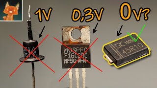
Today we are going to findout which ic is best for our projects tl494 vs SG3525 . as we know SG3525 ic is very popular in various SMPS or high frequency devices . These ics has lots of function. SG3525 The SG3525A, SG3527A pulse width modulator control circuits offer improved performance and lower external parts count when implemented for controlling all types of switching power supplies. The on–chip +5.1 V reference is trimmed to ±1% and the error amplifier has an input common–mode voltage range that includes the reference voltage, thus eliminating the need for external divider resistors. A sync input to the oscillator enables multiple units to be slaved or a single unit to be synchronized to an external system clock. A wide range of deadtime can be programmed by a single resistor connected between the CT and Discharge pins. These devices also feature built–in soft–start circuitry, requiring only an external timing capacitor. A shutdown pin controls both the soft–start circuitry and the output stages, providing instantaneous turn off through the PWM latch with pulsed shutdown, as well as soft–start recycle with longer shutdown commands. The under voltage lockout inhibits the outputs and the changing of the soft–start capacitor when VCC is below nominal. The output stages are totem–pole design capable of sinking and sourcing in excess of 200 mA. The output stage of the SG3525A features NOR logic resulting in a low output for an off–state while the SG3527A utilized OR logic which gives a high output when off. • 8.0 V to 35 V Operation • 5.1 V ± 1.0% Trimmed Reference • 100 Hz to 400 kHz Oscillator Range • Separate Oscillator Sync Pin • Adjustable Deadtime Control • Input Undervoltage Lockout • Latching PWM to Prevent Multiple Pulses • Pulse–by–Pulse Shutdown • Dual Source/Sink Outputs: ±400 mA Peak TL494 is also popular across Computer PSU because it is made to drive Transisters. Complete PWM Power-Control Circuitry • Uncommitted Outputs for 200-mA Sink or Source Current • Output Control Selects Single-Ended or Push-Pull Operation • Internal Circuitry Prohibits Double Pulse at Either Output • Variable Dead Time Provides Control Over Total Range • Internal Regulator Provides a Stable 5-V Reference Supply With 5% Tolerance • Circuit Architecture Allows Easy Synchronization The TL494 incorporates all the functions required in the construction of a pulse-width-modulation (PWM) control circuit on a single chip. Designed primarily for power-supply control, this device offers the flexibility to tailor the power-supply control circuitry to a specific application. The TL494 contains two error amplifiers, an on-chip adjustable oscillator, a dead-time control (DTC) comparator, a pulse-steering control flip-flop, a 5-V, 5%-precision regulator, and output-control circuits. The error amplifiers exhibit a common-mode voltage range from –0.3 V to VCC – 2 V. The dead-time control comparator has a fixed offset that provides approximately 5% dead time. The on-chip oscillator can be bypassed by terminating RT to the reference output and providing a sawtooth input to CT, or it can drive the common circuits in synchronous multiple-rail power supplies. The uncommitted output transistors provide either common-emitter or emitter-follower output capability. The TL494 provides for push-pull or single-ended output operation, which can be selected through the output-control function. The architecture of this device prohibits the possibility of either output being pulsed twice during push-pull operation. The TL494C is characterized for operation from 0°C to 70°C. The TL494I is characterized for operation from –40°C to 85°C. Enjoy Our video for more Info..
Comments