Скачать с ютуб What is PHYSICAL DESIGN FLOW | FULL STEPS | VLSI в хорошем качестве
What is PHYSICAL DESIGN FLOW | FULL STEPS | VLSI
4 года назад
Скачать бесплатно и смотреть ютуб-видео без блокировок What is PHYSICAL DESIGN FLOW | FULL STEPS | VLSI в качестве 4к (2к / 1080p)
У нас вы можете посмотреть бесплатно What is PHYSICAL DESIGN FLOW | FULL STEPS | VLSI или скачать в максимальном доступном качестве, которое было загружено на ютуб. Для скачивания выберите вариант из формы ниже:
Загрузить музыку / рингтон What is PHYSICAL DESIGN FLOW | FULL STEPS | VLSI в формате MP3:
Если кнопки скачивания не
загрузились
НАЖМИТЕ ЗДЕСЬ или обновите страницу
Если возникают проблемы со скачиванием, пожалуйста напишите в поддержку по адресу внизу
страницы.
Спасибо за использование сервиса savevideohd.ru
What is PHYSICAL DESIGN FLOW | FULL STEPS | VLSI
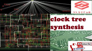
#Vlsi #pnr #cts #physicaldesign #mtech #cadence #synopsys #mentor #placement #floorplan #routing #signoff #asic #lec #timing #primetime #ir #electromigration #interviewquestions #drc #lvs #erc #memory #clock #flipflop #digital #physicalverification #analog #verification #vlsi #companies #vlsi #career #slack #skew #macro #powerplanning #electronics #lowpower #delay #cell #Verilog #STA #UPF #cmos #chip #antenna #intel #silicon #semiconductor #pad #synthesis Physical VLSI design considers the circuit diagram as its input which gets converted into its physical layout. In between there are several important stages to be considered in physical design such as partitioning (decomposition of complex system into distinct subsystem), floorplan( deciding the dimensions and shape of each block in a system design), placement( exact location for blocks in a system) and routing( connection from one block to another) . vlsi design vlsi vlsi design flow vlsi physical design vlsi course physical design static timing analysis design for testability in vlsi asic design flow vlsi design course Tried to explain the full flow of physical design, Starting from synthesis to pnr and upto signoff how it goes.Will explain all the steps detailed in the upcoming videos In integrated circuit design, physical design is a step in the standard design cycle which follows after the circuit design. At this step, circuit representations of the components (devices and interconnects) of the design are converted into geometric representations of shapes which, when manufactured in the corresponding layers of materials, will ensure the required functioning of the components. This geometric representation is called integrated circuit layout. This step is usually split into several sub-steps, which include both design and verification and validation of the layout. Modern day Integrated Circuit (IC) design is split up into Front-end design using HDL's, Verification and Back-end Design or Physical Design. The next step after Physical Design is the Manufacturing process or Fabrication Process that is done in the Wafer Fabrication Houses. Fab-houses fabricate designs onto silicon dies which are then packaged into ICs. Each of the phases mentioned above have Design Flows associated with them. These Design Flows lay down the process and guide-lines/framework for that phase. Physical Design flow uses the technology libraries that are provided by the fabrication houses. These technology files provide information regarding the type of Silicon wafer used, the standard-cells used, the layout rules, etc. Technologies are commonly classified according to minimal feature size. Standard sizes, in the order of miniaturization, are 2μm, 1μm , 0.5μm , 0.35μm, 0.25μm, 180nm, 130nm, 90nm, 65nm, 45nm, 28nm, 22nm, 18nm... They may be also classified according to major manufacturing approaches: n-Well process, twin-well process, SOI process, etc. The main steps in the flow are: Design Netlist (after synthesis) Floor Planning Partitioning Placement Clock-tree Synthesis (CTS) Routing Physical Verification GDS II Generation These steps are just the basic. There are detailed PD Flows that are used depending on the Tools used and the methodology/technology. Some of the tools/software used in the back-end design are : Cadence (SOC Encounter, VoltageStorm, NanoRoute) Synopsys (Design Compiler, IC Compiler, PrimeTime) Magma (BlastFusion, Talus ) Mentor Graphics (Olympus SoC, IC-Station, Calibre) please like share and subscribe to get all the videos. VLSIfab playlist are given below: pnr flow • pnr career guidance in vlsi field. • career guidance in VLSI field Timing and constraints (physical design) • timing and constraints (physical design) M.TECH project IN VLSI • M.Tech Project (schematic to layout)... PHYSICAL DESIGN FLOW IN DIFFERENT TOOLS OF CADENCE AND SYNOPSYS • Physical design flow in different too...
Comments