Скачать с ютуб SCHEMATIC TO LAYOUT (PART2)| VIRTUOSO | CADENCE | VLSI | ASIC DESIGN | VLSIFaB в хорошем качестве
SCHEMATIC TO LAYOUT (PART2)| VIRTUOSO | CADENCE | VLSI | ASIC DESIGN | VLSIFaB
6 лет назад
Скачать бесплатно и смотреть ютуб-видео без блокировок SCHEMATIC TO LAYOUT (PART2)| VIRTUOSO | CADENCE | VLSI | ASIC DESIGN | VLSIFaB в качестве 4к (2к / 1080p)
У нас вы можете посмотреть бесплатно SCHEMATIC TO LAYOUT (PART2)| VIRTUOSO | CADENCE | VLSI | ASIC DESIGN | VLSIFaB или скачать в максимальном доступном качестве, которое было загружено на ютуб. Для скачивания выберите вариант из формы ниже:
Загрузить музыку / рингтон SCHEMATIC TO LAYOUT (PART2)| VIRTUOSO | CADENCE | VLSI | ASIC DESIGN | VLSIFaB в формате MP3:
Если кнопки скачивания не
загрузились
НАЖМИТЕ ЗДЕСЬ или обновите страницу
Если возникают проблемы со скачиванием, пожалуйста напишите в поддержку по адресу внизу
страницы.
Спасибо за использование сервиса savevideohd.ru
SCHEMATIC TO LAYOUT (PART2)| VIRTUOSO | CADENCE | VLSI | ASIC DESIGN | VLSIFaB
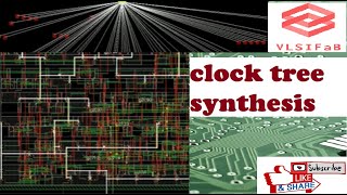
#Vlsi #pnr #cts #physicaldesign #mtech #cadence #synopsys #mentor #placement #floorplan #routing #signoff #asic #lec #timing #primetime #ir #electromigration #interviewquestions #drc #lvs #erc #memory #clock #flipflop #digital #physicalverification #analog #verification #vlsi #companies #vlsi #career #slack #skew #macro #powerplanning #electronics #lowpower #delay #cell #Verilog #STA #UPF #cmos #chip #antenna #intel #silicon #semiconductor #pad #synthesis This is the continuation of my previous video(Nor gate design using full custom flow).In this tutorial, I will be explaining how to make layout directly from the schematic using SCL foundry. If you want to see the continuation of later parts go to the playlist MTech Project. VLSIfab playlist are given below: pnr flow • pnr career guidance in vlsi field. • career guidance in VLSI field Timing and constraints (physical design) • timing and constraints (physical design) M.TECH project IN VLSI • M.Tech Project (schematic to layout)... PHYSICAL DESIGN FLOW IN DIFFERENT TOOLS OF CADENCE AND SYNOPSYS • Physical design flow in different too...
Comments