Скачать с ютуб P-N JUNCTION в хорошем качестве
P-N JUNCTION
10 лет назад
7activestudio
learning
education
cbse
digital
science
medical
diode
zener diode
npn transistor
schottky diode
pn junction diode
diode laser
led diode
semiconductor diode
diode function
transistors
diode theory
vi characteristics of pn junction diode
what is pn junction
semiconductor diodes
junction transistor
pn junction diode characteristics
pn junction diode experiment
transistors for dummies
pn junction animation
Скачать бесплатно и смотреть ютуб-видео без блокировок P-N JUNCTION в качестве 4к (2к / 1080p)
У нас вы можете посмотреть бесплатно P-N JUNCTION или скачать в максимальном доступном качестве, которое было загружено на ютуб. Для скачивания выберите вариант из формы ниже:
Загрузить музыку / рингтон P-N JUNCTION в формате MP3:
Если кнопки скачивания не
загрузились
НАЖМИТЕ ЗДЕСЬ или обновите страницу
Если возникают проблемы со скачиванием, пожалуйста напишите в поддержку по адресу внизу
страницы.
Спасибо за использование сервиса savevideohd.ru
P-N JUNCTION
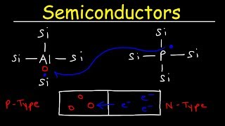
For more information: http://www.7activestudio.com [email protected] [email protected] Contact: +91- 9700061777, 040-64501777 / 65864777 7 Active Technology Solutions Pvt.Ltd. is an educational 3D digital content provider for K-12. We also customize the content as per your requirement for companies platform providers colleges etc . 7 Active driving force "The Joy of Happy Learning" -- is what makes difference from other digital content providers. We consider Student needs, Lecturer needs and College needs in designing the 3D & 2D Animated Video Lectures. We are carrying a huge 3D Digital Library ready to use. P-N JUNCTION: When a p-type semiconductor is suitably joined to n-type semiconductor, the contact surface in called p-n junction. Consider two types of materials: One p-type and the other n-type as show in diagram. Left side material is a p-type semiconductor ‘having negative acceptor’ ions and positively changed holes. The right side material is n-type semiconductor having positive donor ions and free electrons. Suppose the two pieces are suitably treated to form PN junction. Keep in mind that n- type material has a high concentration of free electrons while p- type material has a high concentration of holes. Therefore, at the junction, there in a tendency for the free electrons to diffuse over to the p-side and holes to the n-side. As the free electrons move across the junction from n-type to p-type, positive donor ions are uncovered is they are robbed of free electrons, Hence, a positive charge is built on n-side of the junction. At the same time, the free electrons cross the junction and uncover the negative acceptor ions by filling in the holes. Therefore, a net negative charge in established on P-side of the junction. When a sufficient number of donor and acceptor ions is uncovered, further diffusion is prevented. It is because now positive charge on n-side repels holes to cross from p-type to n- type and negative charge on p-side repels free electron to enter from n-type to p-type. Thus, a barrier is set up against further movement of charge carrier, i.e. holes and electrons. This is called potential barrier or junction barrier v0 The layer name the p-n junction in which no free electrons or holes are available is called the depletion layer.
Comments